Samsung begins mass producing industry’s smallest 14nm DRAM
By applying five EUV (extreme ultraviolet) layers to its 14nm DRAM, Samsung has enhanced the overall wafer productivity by approximately 20% and enabled the industry's highest DRAM bit density. In addition to enhancing productivity, the 14nm process can also help bring down power consumption by nearly 20% compared to the previous-generation DRAM node.

- Country:
- Korea Rep
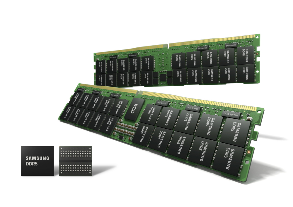
Samsung said on Tuesday it has started mass producing the industry's smallest 14nm EUV DRAM. Based on the latest DDR5 standard, the 14nm DRAM will be ideal for handling ever-growing AI and 5G workloads in data center, supercomputer and enterprise server applications.
By applying five EUV (extreme ultraviolet) layers to its 14nm DRAM, Samsung has enhanced the overall wafer productivity by approximately 20% and enabled the industry's highest DRAM bit density. In addition to enhancing productivity, the 14nm process can also help bring down power consumption by nearly 20% compared to the previous-generation DRAM node.
Samsung says its advanced 14nm DRAM will help unlock unprecedented speeds of up to 7.2 Gbps, which is more than twice the DDR4 speed of up to 3.2Gbps.
Today, Samsung is setting another technology milestone with multi-layer EUV that has enabled extreme miniaturization at 14nm - a feat not possible with the conventional argon fluoride (ArF) process. Building on this advancement, we will continue to provide the most differentiated memory solutions by fully addressing the need for greater performance and capacity in the data-driven world of 5G, AI and the metaverse.
The South Korean firm expects to grow its 14nm DRAM chip density to 24Gb to better meet the rapidly-growing data demands of global IT systems.
- READ MORE ON:
- Samsung 14nm DRAM
- Samsung 14nm EUV DDR5 DRAM
- Samsung


